2018年 10月16日,深圳六碳科技和复旦大学包文中教授团队合作在 Small 上发表论文: High‐Performance Wafer‐Scale MoS2 Transistors toward Practical Application
深圳六碳科技作为作者单位,负责二维材料的制备
Abstract
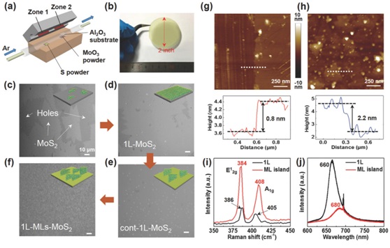
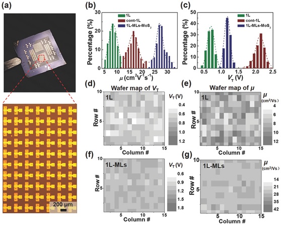
Atomic thin transition‐metal dichalcogenides (TMDs) are considered as an emerging platform to build next‐generation semiconductor devices. However, to date most devices are still based on exfoliated TMD sheets on a micrometer scale. Here, a novel chemical vapor deposition synthesis strategy by introducing multilayer (ML) MoS2 islands to improve device performance is proposed. A four‐probe method is applied to confirm that the contact resistance decreases by one order of magnitude, which can be attributed to a conformal contact by the extra amount of exposed edges from the ML‐MoS2 islands. Based on such continuous MoS2 films synthesized on a 2 in. insulating substrate, a top‐gated field effect transistor (FET) array is fabricated to explore key metrics such as threshold voltage (V T) and field effect mobility (μFE) for hundreds of MoS2 FETs. The statistical results exhibit a surprisingly low variability of these parameters. An average effective μFE of 70 cm2 V−1 s−1 and subthreshold swing of about 150 mV dec−1 are extracted from these MoS2 FETs, which are comparable to the best top‐gated MoS2 FETs achieved by mechanical exfoliation. The result is a key step toward scaling 2D‐TMDs into functional systems and paves the way for the future development of 2D‐TMDs integrated circuits.