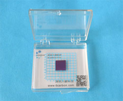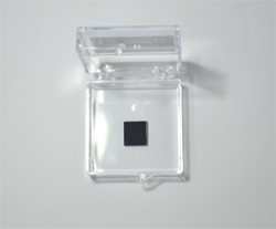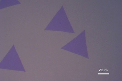
Monolayer triangle MoS2 flakes on SiO2/Si wafer
Size:10mm*10mm (Sale!)
Buy NowSpecifications
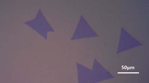
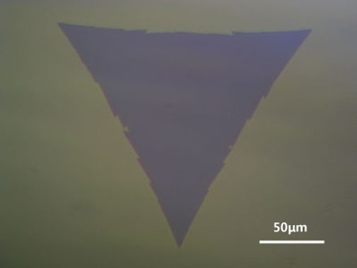
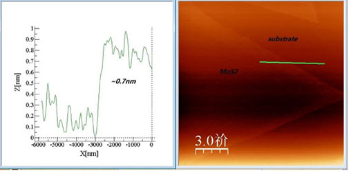
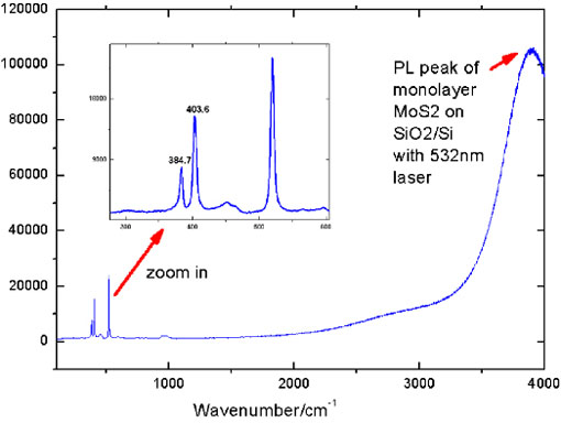
1. The triangle MoS2 is monolayer, single crystalline flakes, and well distributed on the whole surface of the substrate.
2. The flakes size is about 30~120 micrometers.
3. Substrate: 285nm SiO2/Si. Other substrates are available upon requests, such as 100nm SiO2/Si.
4. Larger sizes can be customized. If you have special requests, please contact: sales@6carbon.com
Customization
MoS2 on optical quartz, flexible PET, PDMS, silicon wafer and so on are also provided. Sample size can be customized. Contact sales@6carbon.com and tell us your requirements.
Lead time
In stock. Lead time: 1~3 business days.
Introduction
Molybdenum Disulfide (MoS2) is graphene-like 2D material. One obvious difference with graphene is that MoS2 has a bandgap. Monolayer MoS2 Film is a semiconductor with a direct bandgap of ~1.8eV, while Bilayer or multilayer MoS2 film is has an indirect bandgap decreasing to 1.2eV with layer increase.
6Carbon MoS2 film is produced with chemical vapor deposition (CVD) method, depositing monolayer or multilayer MoS2 Films on various substrates, such as SiO2/Si wafer, Silicon wafer,optical quartz plate,mica, sapphire and so on. We also supply customized MoS2 products based on customers' requirements or design.
Application
MoS2 films are mainly used in optoelectronics fields.