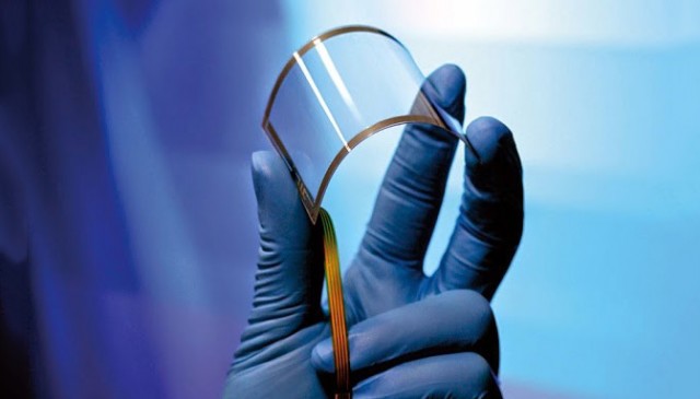
The first fully-2D, wonder-material graphene-molybdenite transistor could be the future of fast electronics
By Sebastian Anthony on June 4, 2014 at 8:39 am | From:http://www.extremetech.com/
Researchers at Berkeley Lab, using a trio of single-atom-thick wonder materials — graphene, boron nitride, and molybdenite – have created the first all-2D field-effect transistor. This FET could also be the first in a new class of electronic devices that are held together with the van der Waals force — the same force that geckos use to walk up a piece of glass. According to Berkeley Lab, these 2D, wonder-material FETs could be the key to a “faster electronics future.”
As you may know if you’ve been following our extensive graphene coverage, graphene is the most conductive material in the world, making it a prime candidate for next-generation electronics. For digital logic, though — actual computation — graphene is useless, because it lacks a bandgap. Fortunately, there’s another monolayer (single-atom-thick) material,molybdenite, that has a perfect bandgap for transistors — and now Berkeley Lab has managed to sandwich both graphene and molybdenite together, to create that mythical all-2D FET. [DOI: 10.1021/nn501723y - "Field-Effect Transistors Built from All Two-Dimensional Material Components"]
In this case, “2D” refers to the fact that the transistor is built entirely out of atomic monolayers. As you can see in the diagram above, this results in a FET that is just six atoms thick. Graphene acts as the gate, source, and drain, hexagonal boron nitride (h-BN) is the gate insulator, and molybdenite (molybdenum disulfide) is the channel. Each layer is a single crystal, with the whole kaboodle being held together by van der Waals force — a weak, intramolecular force (as opposed to more conventional, chemical covalent bonds). This is the same force that we believe is used by a gecko’s feet to scale smooth, vertical surfaces (but in truth, we don’t know a whole lot about van der Waals). [Read: The wonderful world of wonder materials.]
As usual, Berkeley Lab’s 2D FET was produced by way of mechanical exfoliation (a hilarious euphemism for “peeling layers off from a big block using sticky tape). Layers of graphene, h-BN, and molybdenite were laid down on a silicon wafer substrate, and then standard lithography was used to turn it into an actual, functional component. The 2D FET has an excellent on/off ratio, but low to middling electron mobility. Curiously, though, the electron mobility doesn’t decrease at high voltages — which, coupled with the high on/off ratio, could result in some very fast transistors.
“In constructing our 2D FETs so that each component is made from layered materials with van der Waals interfaces, we provide a unique device structure in which the thickness of each component is well-defined without any surface roughness, not even at the atomic level,” says Ali Javey, who led the Berkeley Lab (Lawrence Berkeley National Laboratory) research. “The results demonstrate the promise of using an all-layered material system for future electronic applications.”
Moving forward, Javey and co are faced with the same conundrum that faces much of the current research into wonder materials: How to take that giant step from small-scale, in-the-lab processes (mechanical exfoliation) to large-scale, industrial processes (chemical vapor and atomic layer deposition). Considering recent breakthroughs in mass production of high-quality graphene, we may not have too long to wait.